

 Ask an Expert
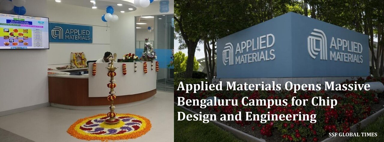
Bengaluru | 27 January 2026: Applied Materials just opened an 8.06 lakh square foot facility at Bengaluru’s International Tech Park, and it is one of the largest semiconductor-focused workspaces in India. This is not an overflowing space where serious chip engineering work happens. The facility consolidates R&D, product engineering, validation, and simulation work.
A Strategic Node for High-Tech Engineering
Applied Materials designs the equipment that makes semiconductor chips, and this centre is handling the complex stuff: designing machinery that manufactures chips at nanometre precision, running validation tests, and building simulation models.
Here’s what makes it technically significant: the centre works directly with Applied Materials’ India Validation Centre, which is the only facility in the country that can process 300mm wafers. That is industry-standard size for modern chip production. The Bengaluru site also connects with Applied Materials’ AI Centre of Excellence in Chennai, creating what amounts to a complete engineering corridor, physical hardware design in Bengaluru, AI and automation work in Chennai.
Bengaluru Still Wins for Semiconductors
Despite all the talk about Tier 2 cities, Bengaluru became the default choice for semiconductor work, and there are real reasons for that.
- Talent density: Nearly 48% of semiconductor job openings in India are in Bengaluru. The city has deep VLSI (Very Large-Scale Integration) skills and people who have worked on chip design projects before. That matters when you’re dealing with equipment that costs millions of dollars and operates on an atomic scale.
- Ecosystem effects: Other semiconductor companies are here. Equipment vendors are here. Testing facilities are here. When something breaks or you need a specialized component, you can get it locally instead of waiting weeks for international shipping.
The infrastructure and ecosystem are already built. You’re not starting from scratch.
“Karnataka remains India’s No. 1 ESDM (Electronics System Design and Manufacturing) hub and a leading chip design cluster.”
– Shri Priyank Kharge, Karnataka’s Minister for Electronics, IT & BT
Avi Avula, President of Applied Materials India, noted the timing matters:
“This investment comes at a pivotal moment for India’s rapidly advancing semiconductor ecosystem.”